- 您现在的位置:买卖IC网 > Sheet目录17337 > ISL6439EVAL1 (Intersil)EVALUATION BOARD 1 ISL6439
�� �
�
�ISL6439,� ISL6439A�
�the� modulator� is� simply� the� input� voltage� (V� IN� )� divided� by� the�
�peak-to-peak� oscillator� voltage� Δ� V� OSC� .�
�Compensation� Break� Frequency� Equations�
�F� Z1� =� ----------------------------------�
�F� P1� =� ---------------------------------------------------------�
�2� π� x� R� 2� x� ?� ----------------------� ?�
�OSC�
�PWM�
�COMPARATOR�
�DRIVER�
�V� IN�
�L� O�
�V� OUT�
�1�
�2� π� ×� R� 2� ×� C� 2�
�1�
�?� C� 1� x� C� 2� ?�
�?� C� 1� +� C� 2� ?�
�F� Z2� =� -------------------------------------------------------�
�F� P2� =� ------------------------------------�
�Δ� V� OSC�
�-�
�+�
�DRIVER�
�PHASE�
�C� O�
�ESR�
�1�
�2� π� x� (� R� 1� +� R� 3� )� x� C� 3�
�1�
�2� π� x� R� 3� x� C� 3�
�Z� FB�
�V� E/A�
�-�
�+�
�ERROR�
�AMP�
�Z� IN�
�REFERENCE�
�(PARASITIC)�
�(EQ.� 5)�
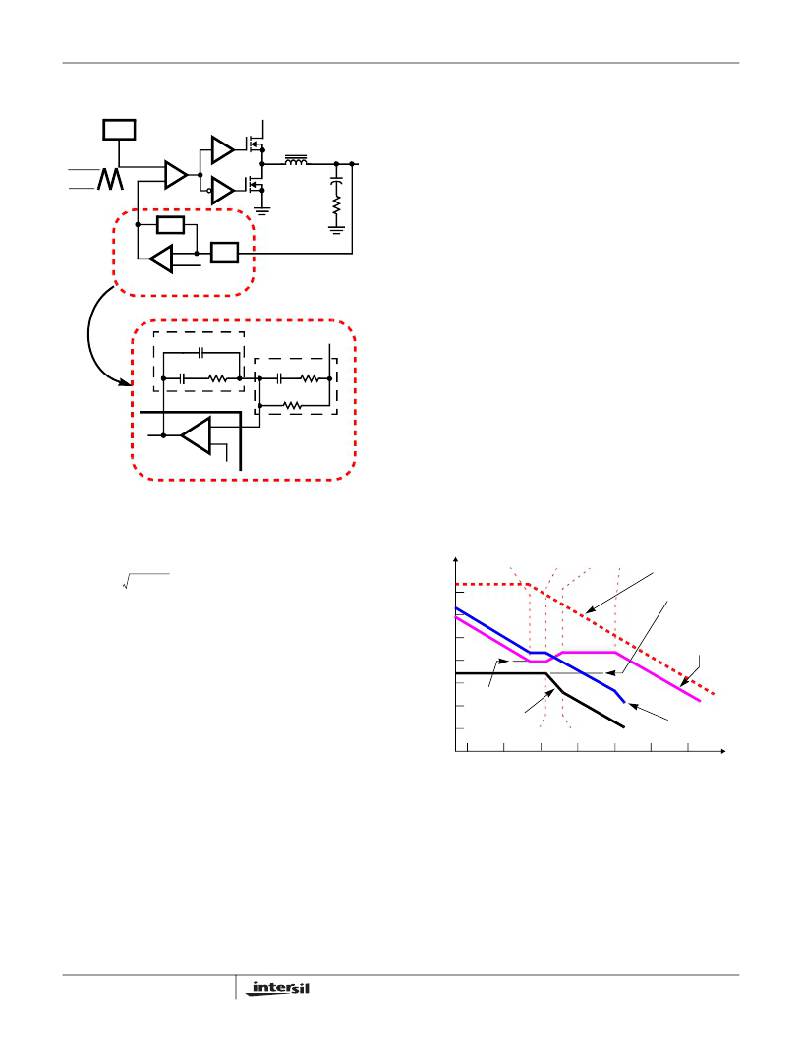
�Figure� 6� shows� an� asymptotic� plot� of� the� DC/DC� converter’s�
�gain� vs� frequency.� The� actual� Modulator� Gain� has� a� high� gain�
�peak� due� to� the� high� Q� factor� of� the� output� filter� and� is� not�
�shown� in� Figure� 6.� Using� the� above� guidelines� should� give� a�
�DETAILED� COMPENSATION� COMPONENTS�
�Compensation� Gain� similar� to� the� curve� plotted.� The� open�
�C� 2�
�C� 1�
�R� 2�
�Z� FB�
�C� 3�
�Z� IN�
�R� 3�
�V� OUT�
�loop� error� amplifier� gain� bounds� the� compensation� gain.�
�Check� the� compensation� gain� at� F� P2� with� the� capabilities� of�
�the� error� amplifier.� The� Closed� Loop� Gain� is� constructed� on�
�the� graph� of� Figure� 6� by� adding� the� Modulator� Gain� (in� dB)� to�
�COMP�
�-�
�+�
�FB�
�R� 1�
�the� Compensation� Gain� (in� dB).� This� is� equivalent� to�
�multiplying� the� modulator� transfer� function� to� the�
�compensation� transfer� function� and� plotting� the� gain.�
�The� compensation� gain� uses� external� impedance� networks�
�ISL6439�
�REFERENCE�
�Z� FB� and� Z� IN� to� provide� a� stable,� high� bandwidth� (BW)� overall�
�loop.� A� stable� control� loop� has� a� gain� crossing� with�
�FIGURE� 5.� VOLTAGE-MODE� BUCK� CONVERTER�
�COMPENSATION� DESIGN�
�-20dB/decade� slope� and� a� phase� margin� greater� than� 45�
�degrees.� Include� worst� case� component� variations� when�
�determining� phase� margin.�
�Modulator� Break� Frequency� Equations�
�F� LC� =� ------------------------------------------�
�F� ESR� =� -------------------------------------------�
�?� V� IN� ?�
�1�
�2� π� x� L� O� x� C� O�
�1�
�2� π� x� ESR� x� C� O�
�(EQ.� 4)�
�100�
�80�
�60�
�F� Z1�
�F� Z2�
�F� P1�
�F� P2�
�OPEN� LOOP�
�ERROR� AMP� GAIN�
�20� log� ?� ----------------� ?�
�?� V� OSC� ?�
�The� compensation� network� consists� of� the� error� amplifier�
�(internal� to� the� ISL6439)� and� the� impedance� networks� Z� IN�
�and� Z� FB� .� The� goal� of� the� compensation� network� is� to� provide�
�40�
�20�
�COMPENSATION�
�GAIN�
�20� log� ?� --------� ?�
�a� closed� loop� transfer� function� with� the� highest� 0dB� crossing�
�frequency� (f� 0dB� )� and� adequate� phase� margin.� Phase� margin�
�is� the� difference� between� the� closed� loop� phase� at� f� 0dB� and�
�180� degrees.� The� expressions� in� Equation� 5� relate� the�
�compensation� network’s� poles,� zeros� and� gain� to� the�
�0�
�-20�
�-40�
�R2�
�?� R1� ?�
�MODULATOR�
�GAIN�
�F� LC�
�F� ESR�
�LOOP� GAIN�
�components� (R� 1� ,� R� 2� ,� R� 3� ,� C� 1� ,� C� 2� ,� and� C� 3� )� in� Figure� 5.� Use�
�-60�
�10�
�100�
�1K�
�10K�
�100K�
�1M�
�10M�
�these� guidelines� for� locating� the� poles� and� zeros� of� the�
�compensation� network:�
�1.� Pick� gain� (R� 2� /R� 1� )� for� desired� converter� bandwidth.�
�2.� Place� first� zero� below� filter’s� double� pole� (~75%� F� LC� ).�
�3.� Place� second� zero� at� filter� ’s� double� pole.�
�4.� Place� first� pole� at� the� ESR� zero.�
�5.� Place� second� pole� at� half� the� switching� frequency.�
�6.� Check� gain� against� error� amplifier� ’s� open-loop� gain.�
�7.� Estimate� phase� margin� -� repeat� if� necessary.�
�10�
�FREQUENCY� (Hz)�
�FIGURE� 6.� ASYMPTOTIC� BODE� PLOT� OF� CONVERTER� GAIN�
�Component� Selection� Guidelines�
�Charge� Pump� Capacitor� Selection�
�A� capacitor� across� pins� CT1� and� CT2� is� required� to� create�
�the� proper� bias� voltage� for� the� ISL6439� when� operating� the�
�IC� from� 3.3V.� Selecting� the� proper� capacitance� value� is�
�important� so� that� the� bias� current� draw� and� the� current�
�required� by� the� MOSFET� gates� do� not� overburden� the�
�FN9057.5�
�November� 5,� 2008�
�发布紧急采购,3分钟左右您将得到回复。
相关PDF资料
695D475X0020D2T
CAP TANT 4.7UF 20V 20% 1810
695D475X0015D2T
CAP TANT 4.7UF 15V 20% 1810
TARS685M025
CAP TANT 6.8UF 25V 20% AXIAL
EBC13DRTI
CONN EDGECARD 26POS DIP .100 SLD
ISL6410EVAL1
EVALUATION BOARD 1 ISL6410
594D226X9020B8T
CAP TANT 22UF 20V 10% 1611
695D335X9025D2T
CAP TANT 3.3UF 25V 10% 1810
RBM10DCTN-S288
CONN EDGECARD 20POS .156 EXTEND
相关代理商/技术参数
ISL6439IB
功能描述:IC REG CTRLR BUCK PWM VM 14-SOIC RoHS:否 类别:集成电路 (IC) >> PMIC - 稳压器 - DC DC 切换控制器 系列:- 标准包装:4,000 系列:- PWM 型:电压模式 输出数:1 频率 - 最大:1.5MHz 占空比:66.7% 电源电压:4.75 V ~ 5.25 V 降压:是 升压:无 回扫:无 反相:无 倍增器:无 除法器:无 Cuk:无 隔离:无 工作温度:-40°C ~ 85°C 封装/外壳:40-VFQFN 裸露焊盘 包装:带卷 (TR)
ISL6439IB-T
功能描述:IC REG CTRLR BUCK PWM VM 14-SOIC RoHS:否 类别:集成电路 (IC) >> PMIC - 稳压器 - DC DC 切换控制器 系列:- 标准包装:4,000 系列:- PWM 型:电压模式 输出数:1 频率 - 最大:1.5MHz 占空比:66.7% 电源电压:4.75 V ~ 5.25 V 降压:是 升压:无 回扫:无 反相:无 倍增器:无 除法器:无 Cuk:无 隔离:无 工作温度:-40°C ~ 85°C 封装/外壳:40-VFQFN 裸露焊盘 包装:带卷 (TR)
ISL6439IBZ
功能描述:IC REG CTRLR BUCK PWM VM 14-SOIC RoHS:是 类别:集成电路 (IC) >> PMIC - 稳压器 - DC DC 切换控制器 系列:- 产品培训模块:Lead (SnPb) Finish for COTS
Obsolescence Mitigation Program 标准包装:2,500 系列:- PWM 型:电流模式 输出数:1 频率 - 最大:275kHz 占空比:50% 电源电压:18 V ~ 110 V 降压:无 升压:无 回扫:无 反相:无 倍增器:无 除法器:无 Cuk:无 隔离:是 工作温度:-40°C ~ 85°C 封装/外壳:8-SOIC(0.154",3.90mm 宽) 包装:带卷 (TR)
ISL6439IBZ-T
功能描述:IC REG CTRLR BUCK PWM VM 14-SOIC RoHS:是 类别:集成电路 (IC) >> PMIC - 稳压器 - DC DC 切换控制器 系列:- 产品培训模块:Lead (SnPb) Finish for COTS
Obsolescence Mitigation Program 标准包装:2,500 系列:- PWM 型:电流模式 输出数:1 频率 - 最大:275kHz 占空比:50% 电源电压:18 V ~ 110 V 降压:无 升压:无 回扫:无 反相:无 倍增器:无 除法器:无 Cuk:无 隔离:是 工作温度:-40°C ~ 85°C 封装/外壳:8-SOIC(0.154",3.90mm 宽) 包装:带卷 (TR)
ISL6439IBZ-TS2705
制造商:Intersil Corporation 功能描述:CISCO, ISL6439IBZ-T W/CONTAINER LABELING - Tape and Reel
ISL6439IR
功能描述:IC REG CTRLR BUCK PWM VM 16-QFN RoHS:否 类别:集成电路 (IC) >> PMIC - 稳压器 - DC DC 切换控制器 系列:- 标准包装:4,000 系列:- PWM 型:电压模式 输出数:1 频率 - 最大:1.5MHz 占空比:66.7% 电源电压:4.75 V ~ 5.25 V 降压:是 升压:无 回扫:无 反相:无 倍增器:无 除法器:无 Cuk:无 隔离:无 工作温度:-40°C ~ 85°C 封装/外壳:40-VFQFN 裸露焊盘 包装:带卷 (TR)
ISL6439IR-T
功能描述:IC REG CTRLR BUCK PWM VM 16-QFN RoHS:否 类别:集成电路 (IC) >> PMIC - 稳压器 - DC DC 切换控制器 系列:- 标准包装:4,000 系列:- PWM 型:电压模式 输出数:1 频率 - 最大:1.5MHz 占空比:66.7% 电源电压:4.75 V ~ 5.25 V 降压:是 升压:无 回扫:无 反相:无 倍增器:无 除法器:无 Cuk:无 隔离:无 工作温度:-40°C ~ 85°C 封装/外壳:40-VFQFN 裸露焊盘 包装:带卷 (TR)
ISL6439IRZ
功能描述:IC REG CTRLR BUCK PWM VM 16-QFN RoHS:是 类别:集成电路 (IC) >> PMIC - 稳压器 - DC DC 切换控制器 系列:- 产品培训模块:Lead (SnPb) Finish for COTS
Obsolescence Mitigation Program 标准包装:2,500 系列:- PWM 型:电流模式 输出数:1 频率 - 最大:275kHz 占空比:50% 电源电压:18 V ~ 110 V 降压:无 升压:无 回扫:无 反相:无 倍增器:无 除法器:无 Cuk:无 隔离:是 工作温度:-40°C ~ 85°C 封装/外壳:8-SOIC(0.154",3.90mm 宽) 包装:带卷 (TR)